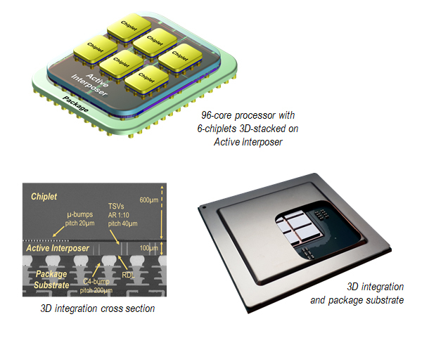
CEA-Leti has announced a new collaboration with Intel on 3D packaging technologies for processors to advance chip design. The research will focus on assembly of smaller chiplets, optimizing interconnection technologies between the different elements of microprocessors, and on new bonding and stacking technologies for 3D ICs, especially for making high performance computing (HPC) applications.
3D technology, which stacks chips vertically in a device, not only optimizes the power of the chip with advanced packaging interconnects between components, but it also allows the creation of heterogeneous integration of chiplets. That ultimately allows fabrication of more efficient, thinner and lighter microprocessors. In addition, by implementing multiple heterogeneous solutions in a single package, chip companies benefit from considerable flexibility, such as mixing and matching different technology blocks with different IP and integrating memory and input / output technologies within the same component. This enables chip makers to continue to innovate and adapt to the needs of their customers and partners.
The key to the work being done by CEA-Leti is to develop new 3D bonding and stacking technologies for integration of devices manufactured in different processes. Speaking to EE Times, Severine Cheramy, the 3D business development director at CEA-Leti, explained the collaboration with Intel is focused on advanced technologies to increase the density of interconnects, and hence decrease the pitch. When asked about the expected outcome of the collaboration, she said she was unable to disclose specific details, but that “we together define a scope of work, technical objectives and deliverables.” She said typically the deliverables might include a technical report and/or some wafers.
Speaking more broadly about the challenges for 3D packaging, she said more advanced research is needed to address issues like production difficulty or simply addressing the cost of implementation. She added, “This collaboration is proof that the electronics world is moving towards advanced packaging and chiplets, and we have some working technology in design flow and test. At a higher level, all the key players working on these advanced packaging technologies need to continue to work together on standardization of interfaces, given that different chiplets from different companies will have different interfaces.”
In 2019, Intel introduced a 3D-stacking technology, Foveros, that adapted these design features. This advanced-packaging technology, launched in Intel Core processors with Intel hybrid technology (codenamed Lakefield), comes in a small physical package for significantly reduced board size to offer an optimal balance between performance and energy efficiency. At the IEEE Electronic Components and Technology Conference in June 2020, CEA-Leti received the best paper award for its work, carried out at IRT Nanoelec, on silicon active interposer as a promising solution towards 3D heterogeneous integration.
Earlier this year, at ISSCC 2020 in February, CEA-Leti presented a paper highlighting its breakthrough in active interposer and 3D stacked chiplets, “A 220GOPS 96-Core Processor with 6 Chiplets 3D-Stacked on an Active Interposer Offering 0.6ns/mm Latency, 3Tb/s/mm2 Inter-Chiplet Interconnects and 156mW/mm2 @ 82%-Peak-Efficiency DC-DC Converters.”


